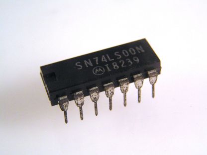
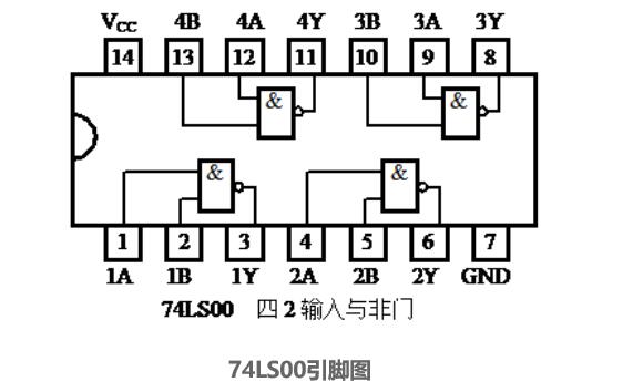
The SN74LS00N is a specific part number for a quad 2-input NAND gate IC from the TTL (Transistor-Transistor Logic) logic family. Here's an overview of its specifications, typical application areas, and methods of implementing logic gate combinations:
Specifications: The SN74LS00N has the following key specifications:
- Supply Voltage (Vcc): Typically operates from a supply voltage range of 4.75V to 5.25V.
- Propagation Delay: The propagation delay is the time taken for the output of the gate to respond to a change in input. The SN74LS00N has a propagation delay in the range of a few nanoseconds.
- Input and Output Logic Levels: The SN74LS00N operates with TTL-compatible logic levels, where a low level (0) is typically around 0.8V or lower, and a high level (1) is typically around 2.4V or higher.
- Operating Temperature Range: The SN74LS00N is designed to operate within a temperature range of 0°C to 70°C.
Application Areas: The SN74LS00N NAND gate can be used in various applications that require logical operations and signal manipulation. Some typical application areas include:
-
Digital Logic Design: The NAND gate is a fundamental building block in digital logic circuits. The SN74LS00N can be used in combination with other logic gates to design complex digital systems like counters, latches, flip-flops, multiplexers, and more.
-
Microcontroller/Processor Interfaces: NAND gates can be used to implement logical functions and signal conditioning between microcontrollers or processors and peripheral devices.
-
Signal Processing: For simple signal processing tasks, NAND gates can be used to perform Boolean operations, multiplexing, demultiplexing, data encoding, or decoding operations.
-
Oscillator Circuits: When combined with other components, NAND gates can form the basis of oscillator circuits for generating clock signals or timing references.
Methods of Implementing Logic Gate Combinations: Logic gate combinations can be implemented using multiple SN74LS00N devices or by using other logic gate families. Some common methods include:
-
Cascading: Multiple SN74LS00N ICs can be cascaded together to form larger logic functions. The output of one gate can be connected to the input of another gate, allowing the realization of complex logic operations.
-
Using Other IC Families: Other IC families like CMOS (Complementary Metal-Oxide-Semiconductor) or other TTL families may be used along with NAND gates to implement specific logic functions. Each IC family has its own specifications and characteristics to consider when designing the circuitry.
-
Programmable Logic Devices (PLDs): Programmable logic devices, such as Complex Programmable Logic Devices (CPLDs) and Field-Programmable Gate Arrays (FPGAs), provide reconfigurable logic functions and can be programmed to implement various logic gate combinations.
-
Integrated Circuit (IC) Packages: There are also specialized IC packages available that combine multiple logic gates into a single package, providing a variety of logic functions in a compact form. These packages are often referred to as standard logic or function-specific ICs.
When implementing logic gate combinations, it is important to refer to the datasheet and documentation of the specific ICs used, as they provide detailed information on pin configurations, truth tables, electrical characteristics, and recommended operating conditions.